


100W RF TR SWITCH (Built & Tested PCB Module)
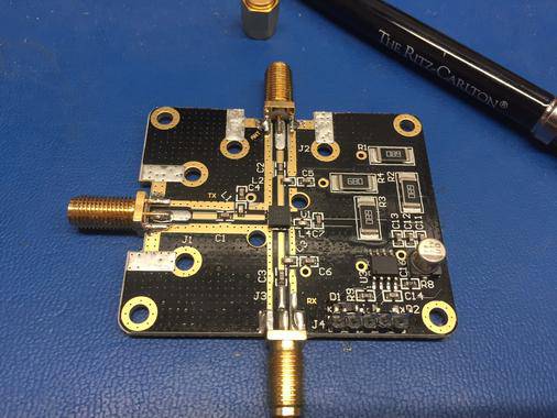
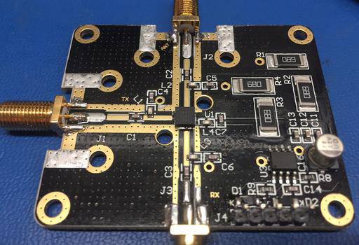
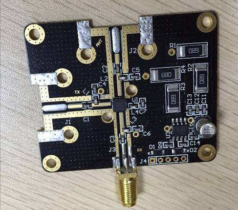
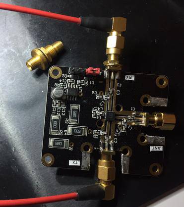
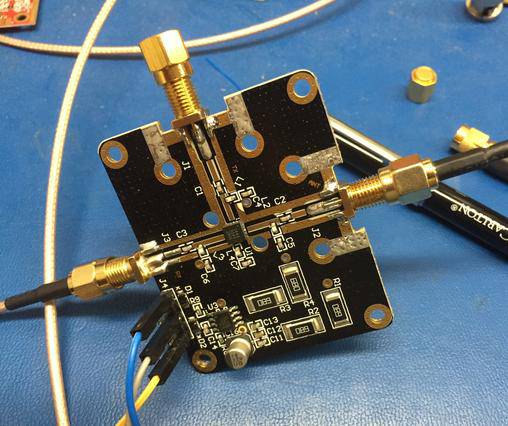
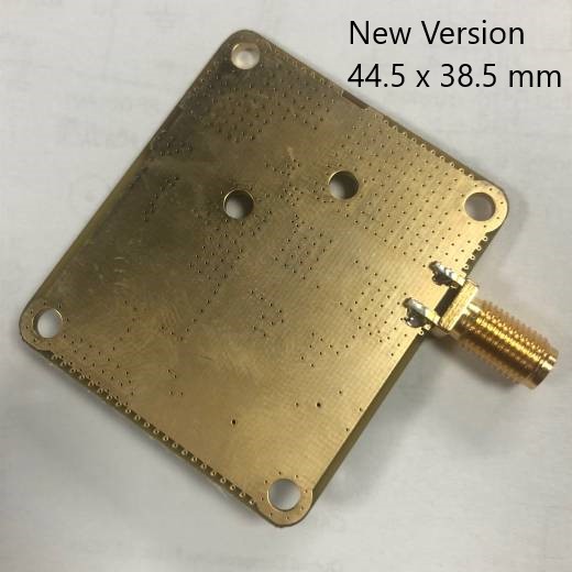
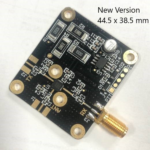
The PCB Module includes a high-quality ENIG R4003 with FR4 4-layer PCB (57 x 48 mm 1.6 mm thick) that comes with all SMD components factory pre-soldered. Special cuts are made for supporting N-type female connectors, for the TX and ANT ports, not supplied together. The RX port female SMA is soldered in place.
RF capacitors are used for all the circuits. High Q inductors are also used. If changed to higher values the frequency response can be shifted to lower frequencies as desired, but I haven't try it yet.
- 50 MHZ - 6 GHZ MACOM PIN Diode IC
- with on-board control interface
- Rogers (TM) R4003 4-layer PCB
A Transmit-Receive Switch (or TR switch) is desirable when we need to connect for example one antenna to a receiver or to a transmitter with frequent change overs. It should have minimum insertion loss between the ports, highest speed of switching and maximum isolation between the ports especially to the receiver port when the antenna connects to the transmitter. A widely adapted solution is to use an electro-mechanical relay, many times a special RF relay (expensive), which has limited life to some 10K...100K operations, it makes noise when operates and sometimes is responsible by itself for failures to unprotected transmitters because of bad or aged contacts. The time delay it introduces, some 10 msec or thereabouts, limits its applications and in addition it is a reason for more damages when a control sequencer is not well designed.
A solid state TR switch can be designed using PIN diodes, or FETs and provide lower cost, no switching noises, good insertion loss, acceptable (manageable) isolation figures and of course virtually endless life. Many HF transceivers use PIN diodes for their TR switch to offer full-break-in (QSK) capability in CW mode. Solid state TR switches are used in RADAR systems and there are applications where the switching rate and switching speed are more important than their isolation or insertion-loss figures.
Today, still, the design of a good solid state TR switch is not easy. Commercial-Of-The Shelf (COTS) T/R switches sell for thousands of USD, depending on power handling, frequency range, switching speed, switching rate, isolation and insertion loss. For example a 30-400 MHZ, 1 KW of power handling and sub microsecond speed at a 2 KHZ rate, sells for many tens of thousands USD. It happened I have worked with some of them in the past for a Frequency Hopping follower jammer project. For best PIN diode performance, many TR switches use high voltage which is generated by DC/DC converters which in turn increase the receiver noise floor and these should be very well designed and applied. And finally, since nearly every device is a non-linear device, 3rd order products are important and is needed to be specified. Even with relays, special low PIM (Passive Inter-Modulation) types are offered just because of the need to reduce IMD products for keeping the system clean and not disturbing other systems.
This design uses a MACOM MASW-000936-14000T IC which contains 3 PIN diodes inside a 4 mm plastic QFN package. It is specified to work from 50 MHZ to 6 GHZ but it needs changing the values of the external components as optimum per the frequency range. My design works well from 230 MHZ to more than 3 GHZ. I have also developed a special driver using only one external chip with MOSFET drivers, normally used for driving larger MOSFETs. It is the IXYS Semiconductor IX4425, which also handles the phase reversed control signal that the MACOM chip needs. By itself, this small chip can supply 4 Amps continuously at high voltage and it is very fast. The MAASW chip needs under 0.5 Amperes, the voltage is not so important, the TR switch works perfectly even with 12V instead of the 28V specified and no DC/DC converter is finally needed, this is good, as we want to avoid any added RX noise. The DC voltage is applied continuously at the ANTENNA port. With the control input left unconnected (it takes a High level through R8) the ANT port gets connected with the RX port with minimum loss (see Photo 4). If the control input goes low, the ANT port connects to the TX port with even lower losses (see Photo 1 and Photo 3). At the same time, a shunt PIN diode shorts out the RX port to increase TX/RX and ANT/RX isolation (see Photo 5). There is a small trick to further improve the isolation figure, by adding another PIN diode at the receiver input. This is how it works. Now, the first implementation had issues and the design presented here is after a second try.
At high power levels, even sub-dB losses are important because they directly translate to heat. For example, a 0.5 dB loss at 100 Watts (50 dBm), means 11 W losses (50 dBm - 0.5 dB = 49.5 dBm = 89 W) which turns to heat which should be managed somehow. The PCB for this design is specially made using 4 copper layers. The top copper layer is on a Rogers (TM) R4003 material in order to stabilize the impedance of the co-planar wave-guide transmission lines, selected over microstrip to minimize coupling, the 1st internal layer is all ground, then there is one FR4 layer and a 2nd internal copper layer which has control routes plus ground, another FR4 layer and finally the last copper layer (bottom) all grounded again. This arrangement, except from the good RF performance, aids spreading the heat off the chip and the power resistors used to bias the PIN diodes to all over the board area. It is like a small heat-sink with 4 fins. The 3 mm holes are for screws used to hold the board into a metal box like the HAMMOND 27134PSLA and between the board and the bottom of the box a special 2 mm thick copper sheet heat spreader can be placed to transfer the heat from the PCB to the box. The copper heat spreader will also move the board upwards so the connector legs and board's pads will not touch the bottom wall. By using this method, one can avoid a special machined box, made for this project.
USING THE TR SWITCH: Before placing this TR switch into your system, it is necessary to plan a sequencer circuit either in hardware or in software. Ensure your antenna has low VSWR. Make sure to cut-off the TX power before operating the switch. Also make sure to first make the switch connect the TX and ANT ports and then apply RF power for transmitting.
For a receiver and transmitter application sharing an antenna, going from receive to transmit,
1. First send the PTT command to transmit to this TR switch only (pin 1 LOW),
2. Then protect your receiver, put the LNA out or check the power level for no damage
3. Then allow your transmitter to generate the signal, or include another switch at the input of your power amplifier for letting the exciter signal to get amplified.
To go from transmit state to receive,
1. First stop generating the transmit signal,
2. Let some time to pass allowing the antenna to unload itself,
3. Then command the TR switch to go to RX, (pin 1 HIGH or leave unconnected)
4. And finally start receiving (put the LNA in or release the PIN diode protection short).
All this sequence can take 10-20 microseconds to complete but be sure and certain of what you are doing in order not to damage the switch or your power amplifier from overshoot or mismatch. If implemented correctly, this TR switch will live a long happy life. If not, the weakest part of your system could be this module and may bring you adventures.
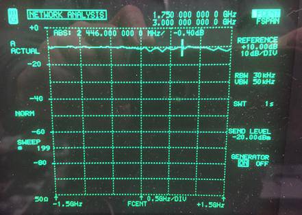
Photo 1.TX port to ANT port frequency response from some KHZ to 1 GHZ. Low loss starts at 230 MHZ. For lower frequencies, one can change the inductors and the DC blocking caps.
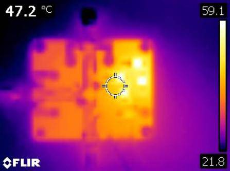
Photo 2.After one hour of operation, the hottest spots are the biasing resistors. Please note, no high RF power is applied and the PCB is not mounted on a heatsink or box.
Photo 3.TX port to ANT port frequency response from 1.25 GHZ to 3.25 GHZ. The ripple shown is partially caused from my measuring cables and imperfect termination. The actual ripple is less than what shown here.
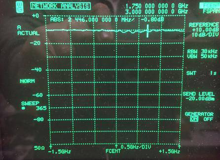
Photo 4. RX port to ANT port frequency response from 1.25 GHZ to 3.25 GHZ. The ripple shown is partially caused from my measuring cables and imperfect termination. The actual ripple is less than what shown here.
Photo 5. RX port to ANT port frequency response from 1.25 GHZ to 3.25 GHZ showing the isolation. The ripple shown is partially caused from my measuring cables and imperfect termination. The actual ripple is less than shown here. The isolation is better than 40 dB all over the frequency range and gets improved with proper termination of the ports.
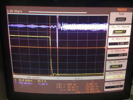
Photo 6.The yellow trace is the TR control signal, 10V for receive, 0V for transmit. The purple trace shows the RF signal at the ANT port.
Photo 7.The yellow trace is the TR control signal, 10V for receive, 0V for transmit. The purple trace shows the RF signal at the ANT port, right on the beginning nanoseconds. The delay since the application of the activation command and the actual RF output is measured to 72 nsec!
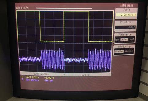
Photo 8.A spectrogram taken with a Tektronix Real Time Spectrum Analyzer to check the TR switch switching rate. This is with 500 usec transmit and 500 usec receive periods.
UPDATE
Looking for better performance on higher frequencies, we cut the N-type section off the PCB and used SMA connectors (see Photo 9) . The insertion loss ripple decreased much (see Photo 10 and Photo 11). Thanks to Nick Perry of MACOM who pointed out to me that the transition on the CPW from the N-type connector was not so good.
Then the TR switch was tested with 100 W of RF power and worked fine! The PCB module was using the box bottom surface as a heat-sink and more sophisticated cooling methods were not found necessary.
Photo 9. The N-type section of the PCB removed and the SMA connectors are now soldered directly on the transmission line.
Photos 10 and 11.The ripple and insertion loss decreased much after removing the N-Type connector PCB section.
UPDATE - 2
Looking for better performance on lower frequencies, we changed values of the capacitors and inductos.
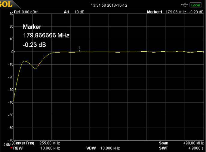
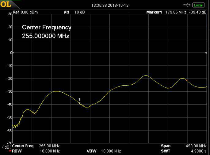
Here is a measurement on 180 MHZ. If you need this modification, please ask for it on a small note when ordering. It offers 0.25 dB insertion loss on transmit and better than 35 dB isolation of the RX port while on TX.