


I2C controlled MF - HF Preselector
- Band-Pass or Band-Reject function
- Continuous 190 KHZ - >30 MHZ tuning
- RF relay switched, without diodes, varactors, small inductors
- 1:1, 4:1 and 16:1 transformers at the input-output to select different bandwidth
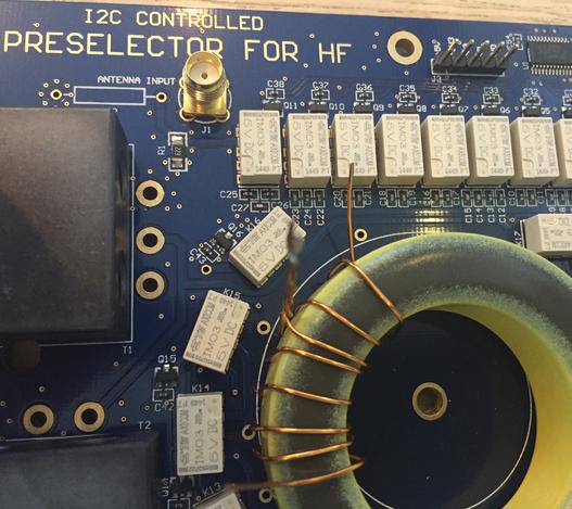
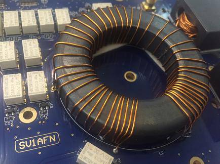
Twenty six RF-type relays, 2 giant toroids, 4 bulky transformers, a large 230 x 105 mm, 3 mm thick PCB, > 6 meters of copper wire, altogether sum to make an "expensive" total, while in the same time most designers aim towards lower cost, size and weight. This is opposite to the "current"... Here is a try just for the optimum. Just what's necessary to make the job done. Thinking of words (cost, optimum, necessary, good engineering etc) kept me busy for days, while discussing to prepare a tunable preselector. Then I thought, we are looking for the lowest phase-noise in frequency synthesizers, the best IMD performance in receiver front-end units, even the best kind of a loudspeaker or head-phones to use with our receiver. And a nice preselector of a good performance is missing, or at least only high-cost xcvrs have one, so I have started making it in order to see how far it can go.
I have checked digitally tuned filters as used on UHF and microwaves, electronic capacitors ICs, ordered some varactors to measure their Q and stability, some cheap inductors to measure IMD, etc. If you are making a good receiver then watch out those cheap inductors they can produce IMD products by themselves, even the toroidal inductors wound on T50 and T68 core size are not good enough and they can jeopardize the performance of an otherwise good design. A preselector is placed just after the antenna and its non-linear qualities should be better than those of a receiver's first mixer.
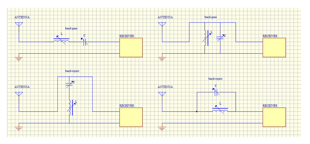
So let's talk about how it works. A capacitor and an inductor have four possible ways to be connected in series or in parallel with the antenna and the receiver input. Two of them make a simple minimal loss band-pass filter and the other two make a band-reject filter. See Fig. 1, below.
Fig. 1. Out of the 4 choises, I have chosen those that do not require ground connection, because the PCB design is hard already and more special attention to the ground loops should be required.
The series tuned circuit, in series with the antenna has been chosen for the band-pass/peaking function and the parallel tuned circuit, in series placed with the antenna has been chosen for the band-reject/notch function. How is this implemented using a relay, is explained in Fig 2.
Fig. 2. The idea of including a switch (DPDT relay) to select band-pass or band-reject
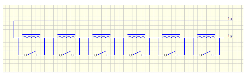
Now, we can make the inductor variable in small steps, like as in Fig. 3 and the capacitor like as in Fig. 4, just like the way automatic antenna tuners are designed. In this design, the variable capacitor assembly synthesizes a value from 0.5 pF minimum up to 1023.5 pF maximum, with a 0.5 pF resolution. The inductor assembly's minimum inductance is 0.625 uH and its maximum is 1280 uH (1.28 mH) with 0.625 uH step. To those values, one should add the pcb stray inductance and capacitance.
Fig. 3. A kind of variable inductor (stepped).
Fig. 4. A kind of variable capacitor (stepped).
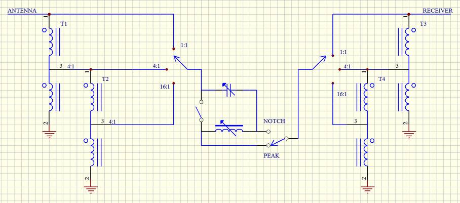
Fig. 5. The complete funtional diagram. It doesn't show the preselector in/out switching which is included on the pcb.
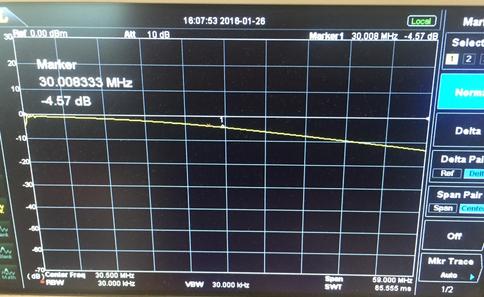
Fig. 3
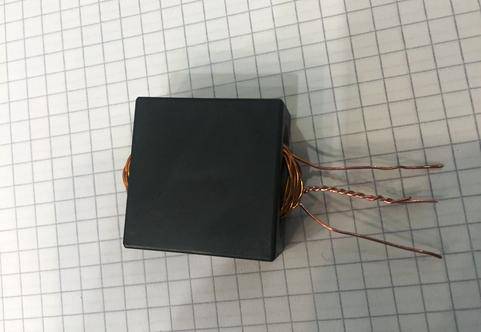
T1-T4 Preparation: Each transformer is wound with 0.5mm diameter enamelled copper wire with 10 bifilar turns. Cut two lengths of 1.20 cm each, twist together to 5-6 turns per inch and count 10 complete U-turns throught the core's two holes.
Separate the twisted wire and identify which winding is the A and which is B using a Ohm-meter. Twist the end of A with the start of B together to make the center.
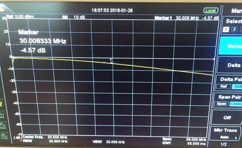
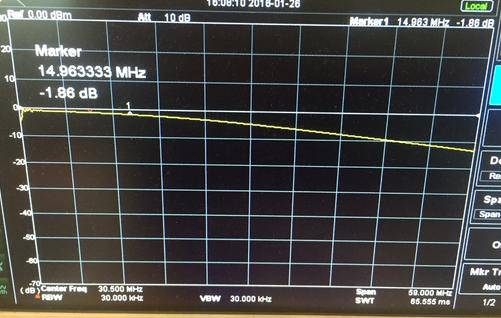
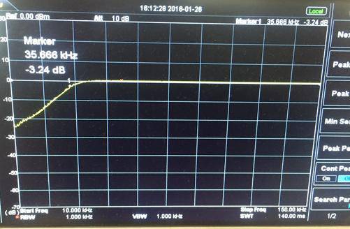
Two of those impedance transformers connected in series have been checked for their frequency response. The -3 dB points are on 33 KHZ and 39 MHZ. The photos show the response of 2 transformers connected together.
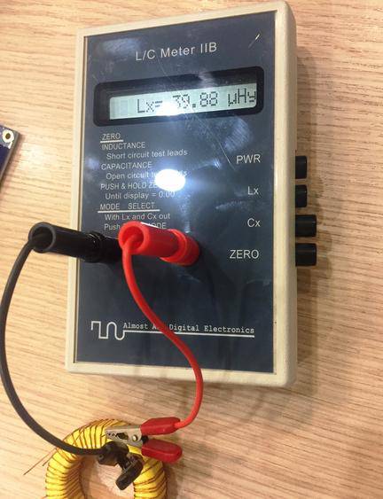
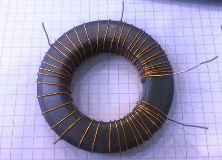
The inductor assembly uses two toroidal cores, one T200-6 for 5.5 - 30 MHZ operation (the -6 material is more stable, it is prefered over the -2 material in VFOs for example) and one FT240-52 ferrite for 140 KHZ - 5.5 MHZ. Adding a third one, like the FT140-77 type, would permit operation down to VLF but I have dropped the idea for cost/size issues plus the ultra low bandwidth and stability problems, one would have to deal with. If someone wants to experiment, then he can place a FT140-77 on the T200-6 position and modify the firmware to make a VLF-5.5 MHZ preselector without changing the FT240-52.
The inductor/capacitor tuned circuit, in series or in parallel connected, is placed between the antenna and the receiver directly using relays, or through 4:1 or 16:1 impedance transformers, one at the antenna end and one at the receiver end. This is to provide a choice for changing the bandwidth of the pass-band (or stop-band) at any time. The bandwidth changes because the impedance adds to the resistance of the inductor of the LC tuned circuit and lowers the quality factor (Q). The transformers change the antenna impedance as it is being seen by the LC circuit, so the LC circuit is loaded with 50 ohms or 12.5 Ohms or 3.1 Ohms, the lower the value, the less is the resistance increase, the narrower is the bandwidth of the tuned circuit as its Q increases. The highest Q position can make a very narrow (sharp) band-pass or notch filter, a few KHZ wide or even less especially towards the lower frequencies. I need to check if the bandwidth decreases so much on LF and MF so it becomes unstable on tuning, i.e., the resonance frequency drifts. Mechanical methods of stabilizing the copper wire turns on the toroidal cores would help for vibrations and covering them with foam will increase isolation from ambient temperature changes.
So the first version of a PCB has been prepared and after winding the inductors correctly so that every tap gives the double inductance of the previous tap, a small controller with OLED display (as used in my RF Attenuator project) with modified firmware can now control the I2C chips which control the relay switching FETs. This controller has an OLED screen and the value of the user set inductance and capacitance can be displayed, together with the calculated tuned frequency. Also, the selection of the band-pass or band-reject function is displayed together with the bandwidth selection and the IN or OUT position. A new controller board is under development which will be equipped with a USB port to read the received frequency from an SDR software (...do they?), an E2PROM to store the last settings before power down, a port to control a cheap DDS chip like the AD9850 or a Si5351A to perform a quick scan over a defined frequency range so if the user has an SDR receiver to visually check the frequency response of the preselector, or make the preselector to tune itself on a fixed frequency as set by the user, adding a AD8310 fast log amp for detecting the rf power after the preselector, some buttons for memory settings of capacitance and inductance values according to the frequency tuned etc. This is another small project but anything like an Arduino can be used. The digital interface is so simple, the progammer needs only to control the I2C chips output pins and update the display.
Since the hardware/software development of the new controller will take a while, I decided to publish the project status as it is today Jan 26th 2016, so fellow hams can communicate and discuss about the final implementation. This idea came up when Ivan, a SWL from Italy, having seen of a Preselector for HF project to be released soon, emailed me about when this project will be available. Today, another one, Bernard from France has asked about the same. He also adviced me to correct some text too. So, you are welcome to share your thoughts using this webpage as soon as I find out how to include a discussion board on this page, first... Till then, you can email me using the form below.