


AD8313 RF Power Detector (Factory Built & Tested PCB Module)
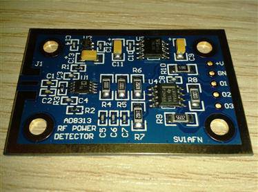
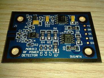
The PCB Module includes a high-quality ENIG FR4 PCB (30 x 45 mm) that comes with all SMD components factory pre-soldered.
RF capacitors are used for all the circuits. A 53.6 Ohm resistor is used for R3.
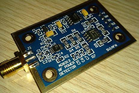
One SMA female connector is also supplied.
With Ultra-Low-Noise Voltage Regulator and 18, 50 and 100 mV/dB Output
Based on the Analog Devices AD8313ARM chip, this module is a complete RF Power meter head for 50 ohm systems
working from below 100 MHZ to more than 2500 MHZ.
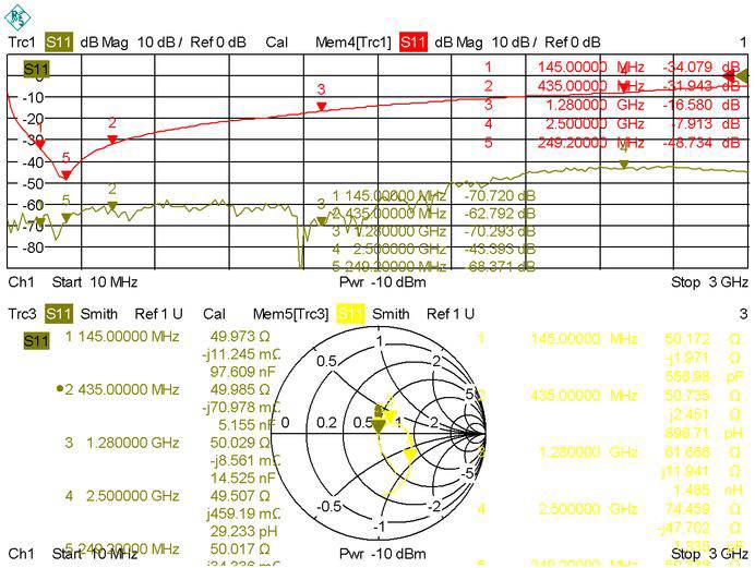
The RF input SMA is terminated to a 53.6 - 1% Ohms resistor (R3) to match the AD8313 input resistance to 50 Ohms.
It draws under 12 mA at 12 VDC and has two internal voltage regulators.
For low noise operation, a special ultra low-noise 3.3 V voltage regulator is used. The TPS79333 is made by Texas Instruments and is optimized for RF circuits. This one powers the AD8313 chip. Its input is connected to an on-board 5 V voltage regulator (LM78L05) to facilitate wide range for the input voltage.
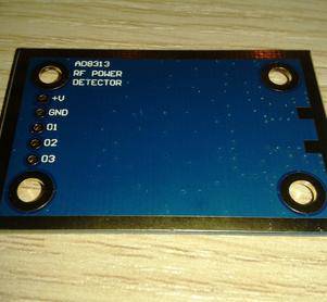
The AD8313 output voltage is routed to the output connector pin 5 for 18mV/dB measurements (O3).
On that route, two 100 nF and one 680 pF capacitors are connected to the ground and can be removed or modified.
Two op-amp DC amplifiers (LM358) multiply the output voltage to 2.77x (50 mV/dB) routed to pin 4 (O2) and to 5.55x (100 mV/dB) routed to pin 3 (O1).
If used, the op-amp chip should be powered by a higher voltage supply (say 12V) in order to be able to deliver higher voltages at higher RF levels.
The op-amp gain scaling resistors are of 1206 size for easier handling if should be changed.
The PCB dimensions are 30 x 45 mm and a special gold-plated band is provided on the edges to help soldering any shielding material (copper clad board, tin etc).
Please note that the current version of boards has a new jumper (J3) to select 3.3V or 5V for the chip operating voltage. Lowering the voltage makes the chip more sensitive to low-power signals but it misses linearity on stronger signals. If you choose to operate at lower voltage, you can use external attenuators to extend the dynamic range. Working at 5V is also possible by placing the J3 jumper at the 5V position.
AD8313 Module S11 measurement kindly conducted and provided by Pierre Binggeli, HB9IAM